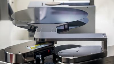
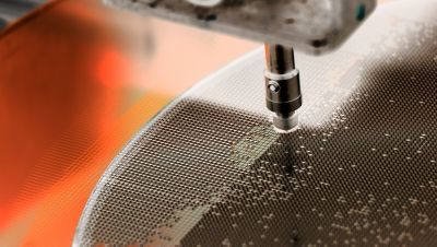
Our advanced inspection solutions detect defects on surfaces, edges, and inside the wafers. We offer defect classification, metrology, and data management to support manufacturers in maintaining quality throughout the wafering process.
With our advanced 2D and 3D inspection systems, we ensure comprehensive quality assurance by inspecting chips individually from wafer to packaging. This guarantees that only flawless components reach the customer and improves traceability and ROI.